TASCAM DA-P20 DAT Deck Low
noise microphone pre-amplifier modifications
Author: Graeme W. Gill
Date: 1994/4/20
Warning:
These modifications are not for the faint of heart.
No responsibility is taken by the author if any of these notes are
incorrect, or you stuff things up. The modifications are electrically
straight forward, but mechanically demanding, as there is not much
space in the recorder to add extra circuitry.
Background:
The TASCAM DA-P20 DAT recorder is (was) an
economical recorder capable of reasonable performance and unlike other
low cost (consumer) DAT records, came equipped with XLR inputs.
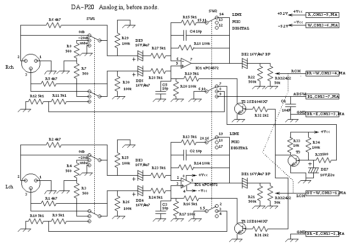
Unfortunately the Microphone input amplifiers have a less than
wonderful noise performance. A look at the circuit diagram quickly
shows why. The differential input amplifier is of the most simplistic
design, using an ordinary op-amp in the standard differential input
configurations. This means that both inputs have a considerable
resistor noise contribution, a contribution equivalent to about 10k
ohms. This is not good.
The modifications described here overcome this problem and give the
DA-P20 a microphone noise performance that is essentially limited by
the op-amp used.
Because of the construction of the input amplifier (lots of surface
mount devices) it is a risky operation to cut tracks. It is also
difficult to back out of the modifications if tracks have been cut. For
this reason I have devised the modifications to completely avoid
cutting tracks.
Components needed:
1 x LM837 Low noise quad
op-amp, in a 14 pin DIP package
1 x NEC PGA2A-05 5 Volt dual reed relay or
equivalent.
1 x BC337 or equivalent npn transistor.
1 x 1N1418 or equivalent small signal diode
4 x 47k resistors
4 x 1k0 1% or better resistors
2 x 47R resistors
1 x 5k6 resistor
1 x 10n bypass capacitor
1/4 watt resistors are satisfactory, but 1/8 watt sized resistors will
make construction easier. The matching of the 1k0 resistors will
determine the Common Mode Rejection Ratio. If you are adventurous you
could try using a lower noise op-amp than the LM837, but you will need
to make sure they are unity gain stable, 4 of them need to fit in a
space not much larger than a 14 pin DIP, and they need to be able to
drive a 600 ohm load. If the op-amp draws its input current the
opposite direction to the LM837 then you will need to reverse the
polarity of DE3 - DE6.
Circuit description:
Here is a circuit diagram of the analog input section before
modification:
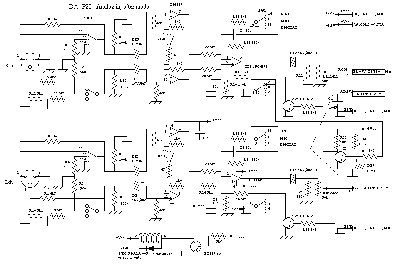
The changes made are:
A differential gain stage is inserted in front of the differential
amplifier already in the DA-P20. The LINE/MIC/DIGITAL switch is
bypassed so that the existing amplifier has a fixed unity gain. The
MIC/LINE gain change is made in the new section by switching the reed
relay. In order to avoid cutting tracks the new gain stage is inserted
in place of the input coupling capacitors, and the gain switching is
done via an inverting transistor relay driver, and spare contacts on
the LINE/MIC/DIGITAL switch.
With the relay open each one of the LM837 op-amps is a unity gain
follower stage. With the relay closed the differential mode gain is
increased to 2000/47 = 32db, while the common mode gain remains at 1.
The input noise voltage is determined by the 47 ohm resistor and the
op-amp noise voltage performance.
Here is the the analog input section after modification:
Removing the analog input PCB:
You need to keep track of which screw came from where, since they vary
in size, length and thread pitch. (Note in particular the screw near
the DC in socket. It looks like the other small black screws, but has a
coarser thread pitch).
1) Eject the cassette carrier, and unclip the cover. It unclips by
moving it towards the front. Push the cassette carrier back into
its closed position.
2) Remove the battery cover and battery.
3) Undo the 12 screws that hold the bottom cover on. With the front
forward there are 3 along the right hand side, 5 on the bottom
(including the one in the recess), 1 on the left hand side and 3 on the
back. Remove the bottom plastic cover.
4) Undo the 5 screws inside that fasten the internal framework to the
top cover (you have to peer past the circuit board to find them). Undo
the 2 screws either side (on the outside) at the front, and the screw
at the DC in socket at the back. Remove the top cover. Watch out for
the eject key falling off.
5) De-solder the 3 green earth leads that attach the front to the
bottom PCB shield. Remove the recording knobs. Gently pry off the front
panel. This will force the volume control knob off, and disconnect two
PCB right angle plugs. Undo the eject switch PCB. Unplug the two front
panel looms. The front panel is now free.
6) The analog input PCB is the one with the record level pot on it.
Undo the screws that hold the PCB shield on to the card. Be careful of
the input selector switch falling off. Loosen the record level pot
collar nut. Undo the two screws that hold the connector plastic and XLR
connectors on. Undo the two loom connectors to completely free the
analog input PCB.
Making the modifications:
There is a limited amount of room and clearance for
the extra components to go onto the PCB, basically the length of SW2,
and not much beyond the edge of the surrounding ground plane outline.
The height of the components should only stick 5mm or so above the
height of SW2.
DE1 and DE2 need to be carefully folded over to lie in the opposite
direction (as indicated by the dotted outline in the layout diagram).
DE7 also needs to lie on its side, and some extra lead length should be
created by heating its pads and drawing it out slightly.
There are two test points circled in the middle of the card, and marked
+V and -V on the layout diagram. The LM837 can both be powered and
supported by these points. I prepared the LM837 by cutting all the pins
except 4 and 11 short, and then bending the short pins slightly
upwards. Pins 4 and 11 are then bent under the IC. These two pins can
be soldered into place to the +V and -V points. The 10n bypass
capacitor can then be soldered between pins 4 and 11. The 1k0 and 47k
resistors are shown spread out in the diagram for clarity, but were
actually mounted vertically. The various interconnections were made
with teflon insulated wire wrap wire. (There is less chance of
accidentally melting the insulation if it is teflon) The ground
connections to the 47k resistors were made by poking the stripped ends
of the wires through the appropriate via holes of R29 and R25 as
indicated in the diagram, and soldering to the ground end of the
resistors.
DE3, DE4, DE5 and DE6 were removed from the PCB, and the +ve lead
carefully bent upwards. The holes closest to the center are used to
connect the outputs of the LM837 (Pins 1, 7, 8 and 14) to the existing
differential amplifier. DE3 - DE6 were put back into the PCB, and the
free (+ve) lead connected to the LM837 inputs (Pins 3,5,10 and 12).
The leads of the relay were cut short and bent outwards, and it was
glued to the top of DE1 and DE2 with a dob of silicon sealer to hold it
in place. The near 1k0 resistors can be connected almost directly to
pins 7 and 8 of the relay, while the 47R resistors with some sleeving
on their leads can connect between pins 1 and 14 of the relay to the
far side 1k0 resistors.
The transistor is mounted upside-down and connected with the 5k6
resistor and diode to pins 2 and 6 of the relay. The emitter of the
transistor can connect to the ground side of DE7, and the +5V can be
got by connecting a wire through the via hole that leads to CN13 pin 5.
On the solder side of the PCB pins 6 & 7, 14 & 15, and 19 &
20 of SW2 need to be connected together. Pins 2 & 4 also need
connecting, and then a wire run from pin 2 to the component side of the
card. I did this by drilling a small hole in the PCB in an area
clear of tracks, near the 5k6 resistor that it needs to connect to.
You need to make sure that there are no shorts, or any chance of
components coming loose. Everything needs to
be kept compact.
The third diagram shows both sides of the circuit card and how the new
circuitry is built and connected:
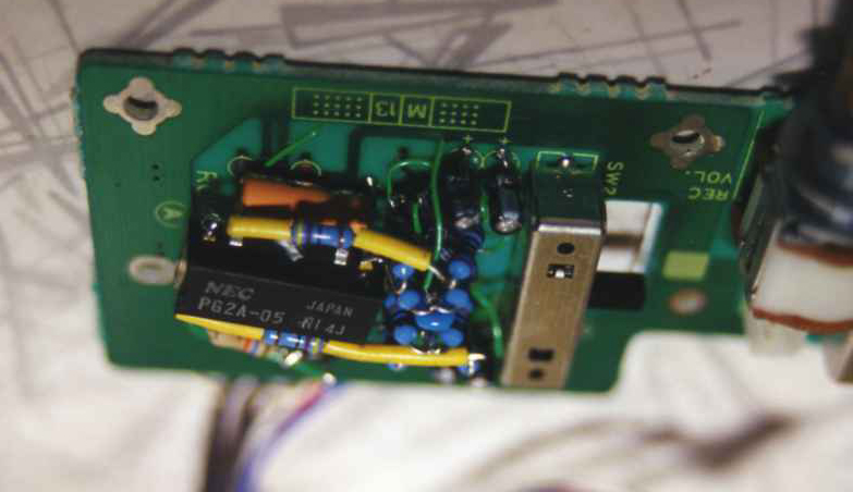
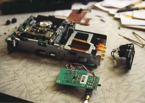
Also here are a couple of photos (Sorry the depth of field is awful):
Testing:
The modifications can be tested by re-connecting the analog input PCB,
plugging the 2 looms back into the front panel, and plugging the back
panel back in. You will need to supply power with the plug pack, and
may have to cover the mechanism with something to stop outside light
upsetting operation.
If everything is working correctly there should be approximately +/-
5.2 volts on the +/- Vcc, 0V on all the outputs of the LM837 and the
uPCV4572,
and if you set the recorder to Pause record and plug a microphone in,
(selecting 0db and Mic of course) the amplifiers should be working
correctly (with a lot less noise than before!). The line level and 20db
pad should also be tested.
Reassembly:
Because all the extra components extend the circuitry closer to the
underlying PCBs, I made up a thin copper U shaped shield that sits in
the frame opening in which the analog input PCB sits. Its edges are
clamped by the PCB, while its insides and outsides were protected from
shorts by covering it with some self-adhesive vinyl sheet.
Re-assembly is then the reverse of the disassembly procedure.
Conclusion:
There you have it. I hope you find this information useful. Feel free
to mail comments, suggestions, praise or news of success. I don't want
to hear of
any failures.
Graeme Gill